
We all know that semiconductor systems are getting more complex, a lot more complex. The burgeoning use of AI in almost everything is certainly accelerating this trend. Faster throughput, lower latency, efficient access to massive amounts of data and the associated communication channels to tie it all together are just some of the challenges faced by chip and system designers. If that’s not enough, the traditional innovation engine for semiconductors – Moore’s Law is slowing. New nodes are harder to get to and the improvement isn’t as large as it has been when you finally do. And extreme complexity means it all doesn’t even fit on a monolithic die anymore. It's something of a perfect storm – a different form of the innovator’s dilemma if you will.
There is a bright spot on the horizon that promises to restore the exponential increases we’ve all come to expect and need. Heterogeneous multi-die design is gaining traction as the way forward. As always, good and bad news here. The good news is that a multi-die approach fueled by a chiplet ecosystem, and a comprehensive design approach can keep the innovation exponential growing. The bad news is that much of the approach is new and is lacking a holistic, cohesive strategy and plan.
Thanks to the aggressive work of the Open Compute Project, there is now a comprehensive plan for how to build a new ecosystem and design paradigm.
GUIDE TO INTEGRATION WORKFLOWS FOR HETEROGENEOUS CHIPLET SYSTEMS
is a new whitepaper that delivers a holistic blueprint for design strategies and ecosystem collaboration. I believe it will become a cornerstone for the next chapter of semiconductor and system development. A link is coming so you can get your copy, but first let’s look at some of the details behind addressing the colossal challenge of system co-optimization with a holistic chiplet design methodology.
About OCP and the Collaboration
The Open Compute Project Foundation is a 501(c)(6) organization which was founded in 2011 by Facebook, Intel, and Rackspace. Its mission is to apply the benefits of open source to hardware and rapidly increase the pace of innovation in, near, and around the data center and beyond. The Open Compute Project (OCP) is a collaborative community focused on redesigning hardware technology to efficiently support the growing demands on compute infrastructure.
The whitepaper was a collaboration across many companies and industry experts. The authoring team is composed of:
- Boon Chong Ang, Intel Corporation
- John Caka, Siemens EDA
- Kevin Cameron, Cameron EDA
- Lihong Cao PhD, ASE (US). Inc
- KK Lin PhD, Applied Materials
- Subramanian Lalgudi PhD, Siemens EDA
- Chieh Lo, ASE (US). Inc
- Mark Malinoski, Siemens EDA
- Tony Mastroianni, Siemens EDA
- Jawad Nasrullah PhD, Palo Alto Electron
- Rajesh Pendurkar PhD
- David Ratchkov, Thrace Systems
- Joe Reynick, Siemens EDA
- Satish K Surana, Intel Corporation
- James Wong, Palo Alto Electron
OCP adhered to a set of tenets for this project. They contemplate a broad impact and are worth repeating here:
Openness: In this whitepaper experts in their fields have contributed open workflows for the benefit of anyone taking the endeavor of integrating chiplets into heterogeneous systems.
Efficiency: This whitepaper strives to improve the efficiency of architects, engineers and manufacturers involved in the integration of chiplets by providing complete reference to the various workflows required to implement heterogeneous systems.
Impact: This whitepaper is the first to describe the entirety of workflows employed in the integration of heterogeneous chiplet systems.
Sustainability: The contributors are hopeful that this whitepaper, being the first of its kind, will benefit the anyone interested in growing the Open Chiplet Economy.
This whitepaper has something for everyone. The piece includes a comprehensive glossary of terms and a detailed definition of the various personas involved in the process. These personas are then referenced in the document to help set the context for collaboration. This document can be used as a comprehensive guide to a new class of innovation.
Here are the topics covered in this important document. You will see that the section titles read like the boxes on a system design flowchart.
Partitioning and Chipletization
Since chiplet-based designs provide a variety of options to improve system performance, power and area tradeoffs, this is a fitting place to start the journey. The elements of a chiplet-based design can be sourced by multiple vendors. This fact demands a well-defined architectural specification and a complete approach to verification. The verification task can become highly complex and so new automated approaches are required.
This chapter discusses co-architecture, co-design, co-optimization and co-verification that requires advanced allocation and partitioning methods and tools. These are referred to as cybertronics design automation.
The discussion goes on to explain that the challenge to designing a cybertronics stack which the functionality can “fit” into is determining how hardware dependent the functionality is. The problem is broken down to hardware dependency in five levels, with level one being the most hardware independent software, and level five being so hardware dependent that the algorithms must be implemented in discrete circuit blocks without software being executed, typically referred to as accelerators. The discussion then focuses on a partitioning method that can address levels three and four, that is the threshold of software meeting hardware to realize system functionality.
Figure 1 proposes a set of contractual functional allocation levels to implement the approach
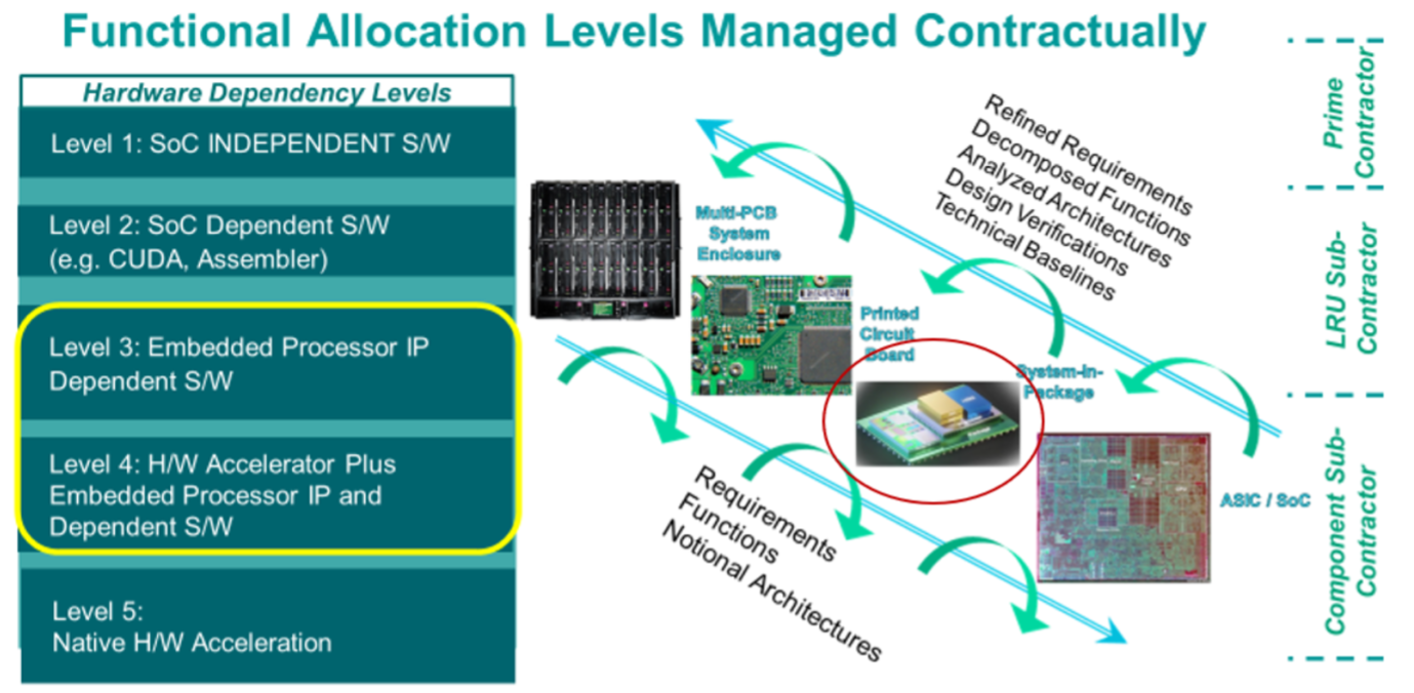
Figure 1. Contractual Functional Allocation Levels. Courtesy Siemens EDA
The graphic at the top of this post, also courtesy of Siemens EDA illustrates the dimensions of solution space exploration. There is a lot more valuable discussion in this section. A link to the unabridged text is coming.
Architectural Planning and Analysis Workflow
This section draws parallels for scaling. Traditional IC design scaling has been accomplished with IC technology scaling, or design-technology co-optimization (DTCO). As the pace of IC technology scaling has dramatically diminished over the past decade, a new process named system technology co-optimization (STCO) is extending design scaling. STCO enables architectural and technology trade-offs early in the system design process to achieve high-performance, cost-effective solutions in a reduced timeframe. It turns out predictive analysis is a fundamental component of STCO that leverages high-level modeling and analysis during the planning phase.
This chapter goes on to define, in detail, the product specification inputs, intellectual property (IP) inputs, and the required output descriptions. Architectural planning and analysis workflows are then described. Items that are addressed here include:
- Micro-Architectural Specification
- SiP (System in Package) RTL Design
- SiP Floor Planning
- Predictive Power Analysis
- Predictive Thermal Analysis
- Predictive Mechanical Stress Analysis
- Die-to-Die Datapath Planning/Signal Integrity Analysis
- Power Delivery Network (PDN)
- System DFT Specification Workflow
Figure 2 summarizes the architectural planning and analysis workflow.

Figure 2. Architectural Planning and Analysis Workflow. Courtesy Siemens EDA
Functional Simulation and Verification Workflow
This section begins by pointing out that, although a lot of design work can be done formally from the software level, functional testing is always required to cover design aspects that cannot be guaranteed correct-by-construction. This includes timing and power that are subject to variability in semiconductor manufacturing and validating that test patterns provide appropriate coverage and limit escapes. Also, chiplets add new problems created by interactions that are not foreseen in designing the individual chips, like noise from power supplies and signal crosstalk in communication.
A detailed flow to address these challenges is then described. It is pointed out that OCP focuses on large software (digital) systems, and how those are allocated into hardware. The components mostly communicate through serial links and parallel data buses, so a lot of the verification is looking at the integrity of that communication, and adequacy of power supplies and cooling. Given the scale of the systems, behavioral modeling or virtualization needs to be used for the computational elements, and “transaction level” methodologies for communication modeling. HiL (hardware in the loop) is also an option when dealing with Chiplets that already exist.
Topics covered in this chapter include:
- Overview of a Methodology with Chiplet Systems
- Defect and Fault Coverage
- Bit Error rate and Clock Domain Crossings
- Simulation and Verification Flow
- Functional Simulation and Verification Plan
- Chiplet-Level Verification
- System-Level Simulation and Verification
- Hardware Validation
- Tape-Out
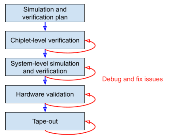
Figure 3. Functional Simulation and Verification Flow. Courtesy Palo Alto Electron
Physical Planning Workflow
This chapter begins with the observation that current packaging technology offers a variety of 2D, 2.5D, and 3D solutions for heterogeneous integration of chiplets to form a product. Choosing the right integration solution will have a significant impact on cost, schedule, and ability to meet performance, functional, and use conditions for the product. Trade-offs include combinations of silicon interposer, organic interposer, substrate, embedded die, die stacking, fan-out technologies, and PCB technologies.
With this backdrop, the following topics are discussed in detail:
- Physical Planning for Chiplet Integration
-
- System Architecture Design
- Chiplet Selection
- Package Selection
- Thermal Analysis
- Power Delivery Network (PDN) Design
- Signal Integrity Analysis
- Package-Level Routing
- Package Manufacturing and Assembly
- Chiplet and Package Interfaces
- Testing and Validation
- Reliability and Quality Assurance
- Software Integration
Power Planning and Analysis Workflow
In this section, the complexity of power for heterogeneously Integrated ICs is discussed. It is pointed out that the complexity of power tree design increases substantially because of the number of power supplies for each component. Careful consideration is needed to determine how power will be delivered to the chiplets - some chiplets may require dedicated power supplies, some die to die interfaces may require power be supplied from another chiplet, and some chiplet power supplies may use a common supply.
In addition, voltage regulator integration into the package creates additional constraints. Due to inefficiencies in voltage regulation, a significant amount of heat is dissipated in voltage regulator ICs. This power dissipation leads to increased heating of the package. Additionally, power management through voltage level modulation needs to ensure that all chiplets can operate at the modulated voltage.
A power modeling and analysis workflow is discussed in detail. It is explained that the power analysis flow serves to provide necessary inputs for thermal, SI/PI and mechanical analysis flows. Most electronic systems are powered by switch-mode power supplies (SMPS), which tend to have an optimum efficiency of around 97% for a narrow band of power; simulation of the system is needed to provide SMPS design requirements.
Chiplet power models are also discussed. These models must account for the following factors:
- Voltage: power dissipation has strong dependence on voltage and operating frequency
- Temperature: in the absence of thermal modeling for the system, models should indicate expected operating temperatures (and allowed excursions)
- Process: basic IC information (thickness, thermal conductivity)
- Modes of operation: all major modes, and (optionally) failing modes. Minor modes optional.
The implications for DFT are also discussed in detail.
Thermal Modeling and Analysis Workflow
This is an area that is heavily influenced by a chiplet approach. Thermal analysis serves to find if any regions of the ICs exhibit high temperatures during normal operation. Typically, temperature limits are based on reliability and performance concerns. A difference in power densities can cause some regions of the die to exhibit higher temperatures than the rest, resulting hot spots.
Integration of multiple ICs in a package allows for bigger and more complex ICs, but also increases the overall power density and concerns about maximum temperatures. In addition, heterogeneous components come with their own maximum temperature limits, e.g. memory modules may have lower maximum operating temperatures than a GPU. In chiplets implementing advanced power management techniques, such as thermal throttling and DVFS, thermal analysis can help answer what, if any, impact the thermal cooling design has on performance.
A detailed thermal modeling and analysis approach is discussed. The flow includes consideration of chiplet operation and power densities, package technology choice, placement options and cooling solution options with the ability to:
- Determine and validate optimal thermal placement
- Determine and mitigate thermal coupling between components
- Determine max components temperatures during operation, e.g. memory, optical, CPU
Since many advanced components, such as GPUs and CPUs implement advanced power and thermal management techniques, detailed thermal analysis is needed to determine actual operational temperatures. Figure 4 illustrates a thermal simulation of a 2.5D chiplet system.
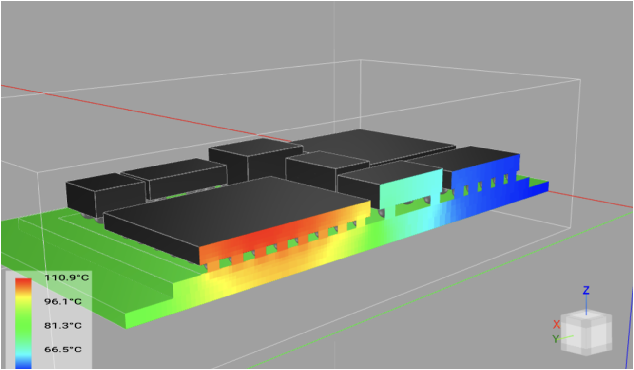
Figure 4. Thermal Simulation of 2.5D Chiplet System. Courtesy Thrace Systems
Signal Integrity and Power Integrity Workflow
As touched on earlier in the whitepaper, there are many partitioning strategies for a chiplet-based design. For example:
- Separate chiplets for core, memory, and IO
- Whether to use the same or different process nodes for chiplets
- Whether to go serial or parallel interface
- What protocol to choose.
There are also several choices for packaging technologies such as substrate-based, interposer-based, or RDL fanout-based. And so there are several possible design scenarios that need to be analyzed to find the optimal choice. Signal and power integrity play a major role here and this chapter dives into the types of evaluation and analysis that inform the best system design decision.
For example, specifications for power dissipation, latency, data rate, bandwidth, packaging technology, and cost must be defined for each micro-architecture. Predictive signal integrity analysis is done to check the die-to-die performance against minimum functional specifications.
There is a great deal of detail in this section. Some of the expected results of this work include:
- Determine if die-to-die interfaces in a given micro-architecture are in compliance with their respective signal integrity functional specifications
- Determine the optimal configuration (placement, trace width, etc.) for a given micro-architecture that best meets the signal integrity functional specifications
- Determine the optimal micro-architecture that meets the signal integrity functional specifications
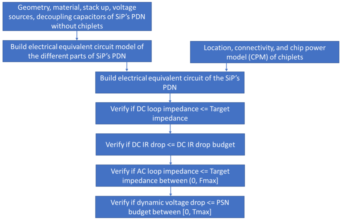
There are many flows described in this section. Figure 5 illustrates a predictive power integrity simulation workflow for a SiP
Figure 5. Flowchart describing the predictive power integrity simulation workflow for a SiP.
Licensed under a Creative Commons Attribution-ShareAlike 4.0 International
This chapter provides a simplified summary of existing STA tools and workflows and discusses new tools and workflows required to adapt the methodology for SiP-level analysis.
For large SiP-level designs, it is pointed out that a full gate-level STA timing approach will most likely be prohibitive. As such, an analogous, hierarchical approach can be deployed treating each of the chiplets as “blocks” and the SiP-level analysis will focus on top level, chiplet-to-chiplet, low speed interfaces. This methodology will require a simplified .LIB model to be created for each of the chiplets primarily focused on the chiplet input/output timing constraints.
Approaches for both 2.5 and 3D designs are presented. In 2.5D designs, there are many different packaging technologies used to implement the die-to-die interconnect. Silicon and/or organic substrate/interposer materials can be used, which require different extraction tools and workflows. A key point is that a hybrid, silicon/organic parasitic extraction workflow is required to support 2.5D STA analysis.
For true 3D digital IC designs, traditional ASIC level STA methods for both die level and die-to-die level timing analysis will be deployed. But changes will be required to accommodate the new hybrid bonding die-to-die interconnect and muti-ASIC technology nodes.
Figure 6 illustrates a high-level summary of a 2.5D, SiP-level STA workflow.

Figure 6. Flowchart Describing SiP-Level STA Workflows. Courtesy Siemens EDA
Mechanical Analysis Workflow
This chapter describes the truly new and highly demanding requirements for mechanical analysis of chiplet-based designs. The chapter explains that technical modeling and analysis are key enabling technologies for chiplet Integration that will support product development across the chip-package-board-system domains.
It is observed that analysis using modeling and simulation tools today are mainly applied for a single mechanical domain (die, package or board/system). The future will require multi-physics and scale capabilities as well as design collaboration (die-package-board/system). Mechanical modeling and simulation tools will also be required to support development of both process and assembly design kits (PDK and ADK).
To motivate the discussion, it is pointed out that mechanical reliability concerns are more elevated in a chiplet-based design than in a monolithic SoC for the following reasons:
- Heterogeneous Integration: Chiplet-based designs typically involve integrating multiple chips from different suppliers or with varying technologies. This can lead to differences in material properties, thermal coefficients, and mechanical behaviors, making it more challenging to ensure uniform mechanical reliability across the system.
- Interconnection Complexity: In chiplet-based designs, there is a need for numerous interconnections between chips, such as through-silicon vias (TSVs), micro bumps, and solder joints. These interconnections are susceptible to mechanical stresses, including thermal expansion mismatches and mechanical shock, which can lead to reliability issues like solder joint fatigue, cracking, and delamination.
- Thermal and Power Challenges: The thermal and power challenges in chiplet-based designs can be more prominent due to non-uniform temperature distribution among the chiplets leading to thermal hotspots and gradients that can exacerbate mechanical stress and reliability concerns.
- Packaging Complexity: The packaging of chiplet-based designs must account for multiple chips, each with its own mechanical properties and requirements. This complexity can lead to mechanical inconsistencies. These variations can result in uneven mechanical stress distributions and affect long-term reliability.
A detailed mechanical analysis flow is then described. Figure 7 provides an overview of an example flow.
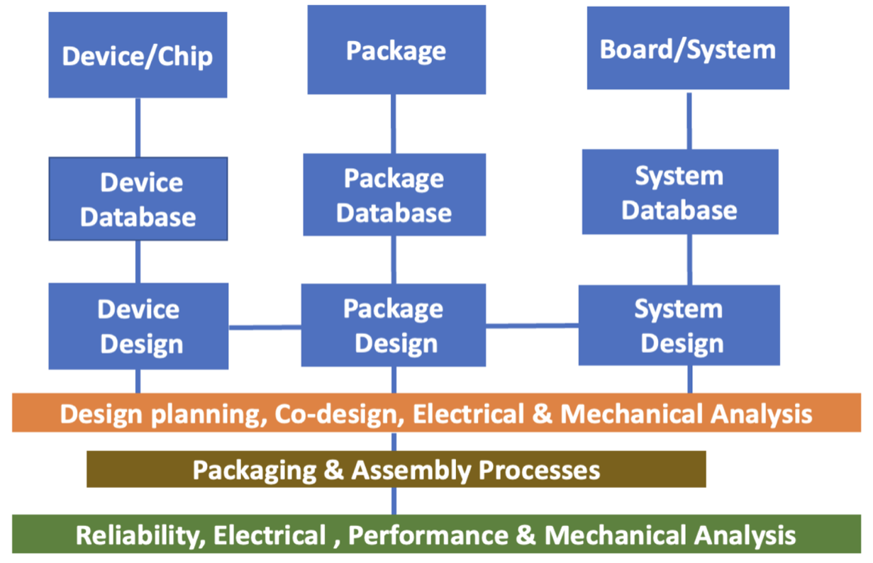
Figure 7. Mechanical Analysis for Chiplets Integration. Courtesy ASE USA Inc.
Test Workflows for Multi-Die System-in-Package
This final chapter covers the recommended workflows for testing chiplet-based system-in-package (SiP) designs. A tool-generic 3D workflow for DFT, IP, and wafer, and SiP package test is discussed.
The chapter begins with chiplet test planning considerations, then moves to DFT and IP test implementation at the die level. Planning concepts include coordination with other dies in the package, and test access methods. Then, known-good die (KGD) wafer probe DFT and IP test requirements and techniques are discussed, including micro bump test access considerations.
System-in-package (SiP) testing after die/package assembly is next. Topics for SiP package test include die-to-die (D2D) interconnect test and repeating the KGD DFT and IP tests at the package level, including die-level test vector application from the package pins.
The chapter concludes with system-level test with the fully tested and packaged parts at the board level. Topics include interconnect testing, along with DFT and IP test access at the board and system levels. Throughout the discussion, test-related package, power, thermal, reliability and test hardware requirements are highlighted. As an initial overview, SiP challenges compared to a very large SoC include:
- Higher power density, IR drop, and noise
- Thermal load and cooling issues
- Lower package yield due to increased packaging steps and complexity
- The requirement that dies must be fully tested at wafer probe before packaging
- Wafer probe is more difficult for SiP chiplets and SoCs than for standard ICs
There are many aspects of testing at the various levels of integration covered in detail. Like the rest of this whitepaper a complete blueprint is presented. Topics covered in this chapter include:
- 2.5D Design Overview
- Multi-Die Test Planning
- DFT in 3D Designs
- 3D DFT Workflow
- Purpose of the Multi-Die Flow
- Expected Results
- Flowchart
- Wafer Probe Manufacturing Test
- Package Manufacturing Test
- IP Manufacturing Test
- Other Tests, such as high temperature operating life (HTOL), failure analysis, and corners analysis
Figure 8 illustrates a 3D test insertion workflow.
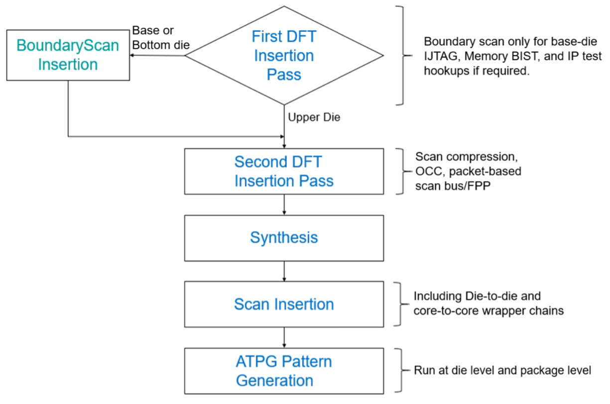
Figure 8. 3D DFT Insertion Flow. Courtesy Siemens EDA
To Learn More
This whitepaper provides a detailed exploration of the evolving landscape for chiplet-based system design. The strategies and tactics proposed mark a substantial shift from traditional SoC methodologies. The entire lifecycle of system design must be optimized for this approach to work. Chiplet design and packaging manufacturing opens a new chapter for semiconductor development. One that counteracts the deceleration of Moore's Law and the constraints associated with large, monolithic SoCs.
As such, the effort to achieve a new methodology and ecosystem is clearly worth it. The methodologies and insights presented in this whitepaper are foundational for achieving this goal. This document serves as an essential guide and reference for professionals and enthusiasts in the field. The future of chiplet-based design is bright, with vast opportunities for technological breakthroughs.
Download your copy of this important document here, and begin to understand the details behind addressing the colossal challenge of system co-optimization with a holistic chiplet design methodology.